Until the formation of the inversion layer at the MOS interface 2
Continuation of the article explaining the charge state until the inversion layer is formed at the MOS interface. Consider the case where an oxide film and a metal electrode are formed on a Si p-type semiconductor. The formation of an inversion layer at the MOS interface when a voltage is applied is divided into the following four cases.
0. Electrodes and semiconductors at 0V
1. A state in which + voltage is applied to the electrode side and - voltage is applied to the
semiconductor side (depletion is progressing)
2. A state in which + voltage is applied to the electrode side and - voltage is applied to the
semiconductor side (depletion stops and an inversion layer is formed)
3. A state in which + voltage is applied to the electrode side and - voltage is applied to the
semiconductor side (the charge in the inversion layer increases)
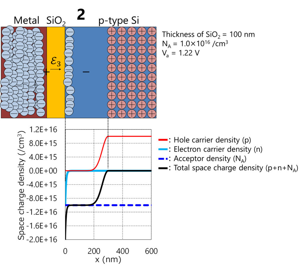
2. A state in which a + voltage is applied to the electrode side and a - voltage is applied to the semiconductor side (depletion stops and an inversion layer is formed)
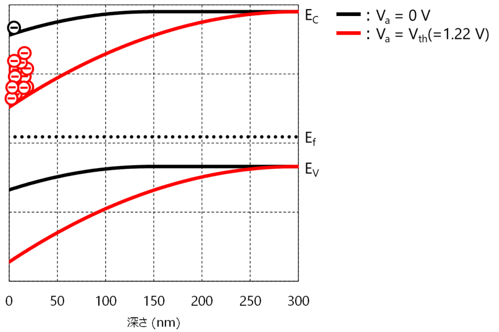
As shown in the band diagram below, when the threshold voltage is reached, the electron carrier density increases rapidly as \(E_C\) approaches the Fermi energy. Below the threshold voltage, few electrons exist at the interface due to the large difference between \(E_C\) and \(E_f\). Therefore, when the voltage is below the threshold voltage, the depletion layer is widened to maintain the charge balance between the electrode side and the Si side.

* Threshold voltage = the voltage at which the electron carrier density at the interface between the semiconductor and the oxide film becomes the same value as the acceptor concentration.
The space charge density when reaching the threshold voltage is shown below. It can be seen that the electron carrier density is high only at the interface between the semiconductor and the oxide film. (The specific calculation method will be explained separately.)

3. A state in which a + voltage is applied to the electrode side and a - voltage is applied to the semiconductor side (the charge in the inversion layer increases)
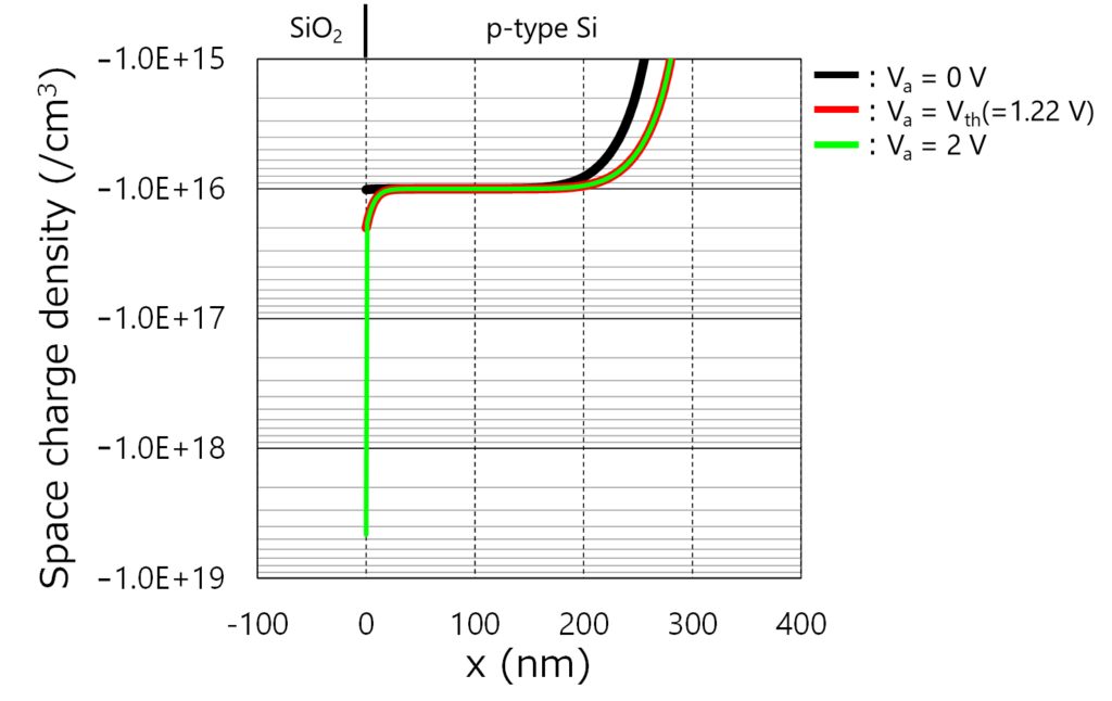
A large number of electrons gathered at the interface prevents the depletion layer from expanding any further. When the voltage is slightly increased, the charge on the surface increases exponentially, and the electric field across the oxide film increases, so the depletion layer does not extend. It may be considered that only the interface between the semiconductor and the oxide film becomes metal. The electric field at the interface becomes larger than that at the depletion layer. Therefore, even if the voltage is increased, electrons are attracted to the interface and the depletion layer does not expand. The figure below shows the results of calculating the space charge density assuming that the charge accumulates at a point of 1 nm on the interface. Above the threshold voltage, only the charge at the interface increases and the depletion layer does not spread.

Since we are considering the MOS interface, the description is somewhat complicated. However, since \(E_f\) ≒ \(E_C\) after the formation of the inversion layer, if we consider it to be the same as a metal, we simply sandwich the oxide film between the metals. That's a matter of course, as the electric field increases, the charge builds up at the interface. However, charges cannot be accumulated infinitely at the oxide film interface. When the electric field in the oxide film reaches the dielectric breakdown electric field, the oxide film breaks down and cannot store charges.
Referenced literature
Nothing special. Created based on my experience.